


Mastering PCB Layout: The Art and Science of Circuit Board Design

Designing a printed circuit board (PCB) is both an art and a science. It requires a blend of creativity, technical expertise, and attention to detail to create a functional and efficient circuit board. In this blog, we’ll delve into the intricacies of mastering PCB layout, exploring the key elements, best practices, and tools that contribute to successful circuit board design.
Understanding PCB Layout
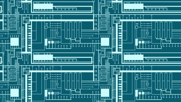
At its core, PCB layout is the arrangement of electronic components, traces, and other elements on a circuit board. The layout directly impacts the functionality, performance, and manufacturability of the final product. Here are some essential aspects to consider:
- Component Placement: Strategically placing components such as resistors, capacitors, integrated circuits, and connectors is crucial for optimal circuit performance and signal integrity. Factors like thermal management and signal routing paths should also be considered during placement.
- Signal Integrity: Ensuring signal integrity involves minimizing signal distortion, crosstalk, and electromagnetic interference (EMI). Proper layout techniques, such as controlled impedance routing and ground plane design, play a significant role in maintaining signal integrity.
- Power Distribution: Efficient power distribution is essential for supplying voltage and current to different components on the board. Proper power plane design, decoupling capacitors, and voltage regulation circuits contribute to stable power delivery.
- Routing Considerations: Routing traces between components requires careful planning to avoid signal interference, meet electrical requirements, and minimize signal propagation delays. Differential pair routing, high-speed signal routing, and signal layer stackup are critical considerations.
Types of PCBs
These are the types of Printed Circuit board
Single-layer PCBs
These have components and circuits on one side of the board, suitable for simpler electronics like calculators or LED displays.
Double-layer PCBs
These have components and circuits on both sides, connected through plated through-holes or vias. They are used in more complex devices like automotive electronics or consumer gadgets.
Multi-layer PCBs
These have multiple layers of conductive material separated by insulating layers (cores and prepregs). They are used in high-performance electronics such as computers, smartphones, and medical devices.
Flexible PCBs
Made of flexible polymer materials, these PCBs can bend or twist. They are used in applications where space or flexibility is crucial, like in wearable technology or aerospace.
Rigid-Flex PCBs
These combine rigid and flexible PCBs, offering both structural integrity and flexibility. They are used in devices that need both durability and adaptability, such as foldable smartphones or medical implants.
The PCB Layout Process
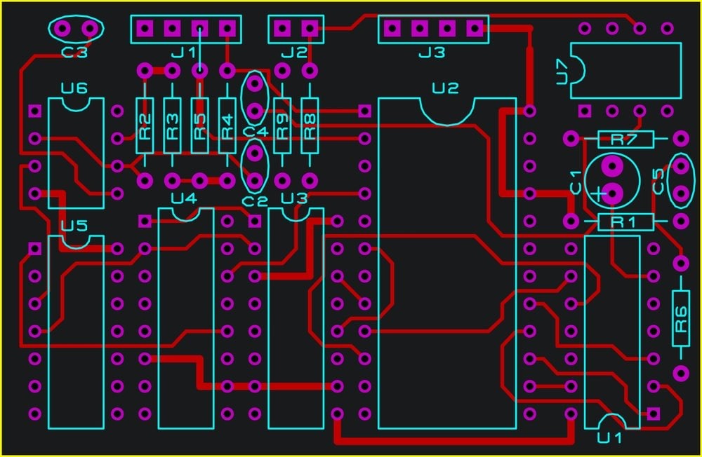
The PCB layout process involves several key steps to ensure a functional and efficient circuit board design:
- Schematic Design: Begin by creating a schematic diagram of the circuit using specialized software. This diagram represents the interconnections between components and their functions.
- Component Placement: Once the schematic is complete, place the components on the PCB layout software. Consider factors like signal flow, thermal management, and ease of assembly.
- Routing Traces: Connect the components using copper traces on the PCB. Route traces carefully to avoid signal interference, optimize signal integrity, and meet design specifications.
- Ground and Power Planes: Designate areas for ground and power planes to ensure stable power distribution and minimize electromagnetic interference.
- Signal Integrity Checks: Conduct signal integrity checks to ensure that signals meet timing requirements, have controlled impedance, and are free from noise or crosstalk.
- Design Rule Check (DRC): Perform a design rule check to verify that the layout complies with manufacturing and assembly guidelines, including clearance, trace width, and minimum hole size.
- Gerber Files Generation: Generate Gerber files, which contain information about PCB layers, traces, pads, and other design elements. These files are used for manufacturing the PCB.
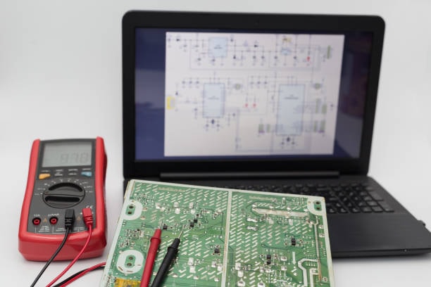
- Prototype Testing: Fabricate a prototype of the PCB for testing and validation. Conduct electrical tests, functional tests, and thermal analysis to verify the design’s performance.
- Design Iteration: Based on test results, iterate the design if necessary to address any issues or optimize performance.
- Final Documentation: Prepare final documentation, including assembly drawings, bill of materials (BOM), and manufacturing specifications, for mass production of the PCB.
Throughout the PCB layout process, collaboration between design engineers, PCB manufacturers, and testing teams is crucial to ensure a successful and reliable circuit board design.
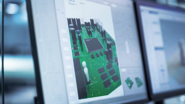
PCB Layout Software
PCB layout software plays a crucial role in designing and optimizing printed circuit boards. Here are some popular PCB layout software tools widely used in the industry:
Altium Designer
Known for its comprehensive features, Altium Designer offers schematic capture, PCB layout, simulation, 3D modeling, and collaboration tools in a unified platform.
Cadence Allegro
Cadence Allegro is a powerful PCB design tool that provides advanced routing capabilities, signal integrity analysis, design rule checks, and integration with other CAD tools.
Mentor Graphics PADS
PADS by Mentor Graphics offers an intuitive user interface, efficient PCB layout tools, high-speed routing capabilities, and design validation features.
KiCad
KiCad is an open-source PCB design software with a strong community and a wide range of features, including schematic capture, PCB layout, 3D viewer, and design rule checking.
OrCAD PCB Designer
OrCAD PCB Designer is a comprehensive toolset for schematic design, PCB layout, simulation, and design collaboration, suitable for complex electronic designs.
Eagle PCB
Eagle PCB by Autodesk is widely used for small to medium-sized PCB designs, offering schematic capture, PCB layout, autorouting, and integration with manufacturing tools.
PADS Professional
PADS Professional is a scalable PCB design software with features like high-speed routing, constraint management, thermal analysis, and collaboration capabilities.
DesignSpark PCB
DesignSpark PCB is a free PCB design tool with a user-friendly interface, schematic capture, PCB layout, 3D viewer, and integration with component libraries.
Best Practices for PCB Layout

To master PCB layout effectively, follow these best practices:
- Use PCB Design Software: Utilize advanced PCB design software like Altium Designer, Eagle, or KiCad, which offer features such as schematic capture, layout tools, design rule checks (DRC), and simulation capabilities.
- Follow Design Guidelines: Adhere to design guidelines provided by component datasheets, industry standards (e.g., IPC standards), and PCB manufacturers. Pay attention to clearance, trace width, via size, and layer stackup recommendations.
- Optimize Component Placement: Group related components together, minimize trace lengths, and place critical components strategically for ease of assembly, testing, and maintenance.
- Route Signals Carefully: Route high-speed signals with controlled impedance routing techniques, use differential pairs for data lines, and minimize signal loops to reduce EMI and signal degradation.
- Consider Thermal Management: Incorporate thermal vias, heatsinks, and proper copper pour techniques for effective heat dissipation, especially in high-power or temperature-sensitive applications.
- Perform Design Validation: Conduct design validation through simulations, prototyping, and thorough testing to ensure the PCB meets performance, reliability, and manufacturability requirements.
Tools and Resources
Several tools and resources can aid in mastering PCB layout:
- PCB Design Software: As mentioned earlier, use professional PCB design software for schematic capture, layout, simulation, and design validation.
- Component Libraries: Access comprehensive component libraries from manufacturers and online repositories to simplify component selection and placement.
- Design Guides and Standards: Refer to industry standards such as IPC-2221 for design guidelines, stackup recommendations, and manufacturing tolerances.
- Online Communities and Forums: Engage with PCB design communities, forums, and online tutorials to learn from experienced designers, seek advice, and stay updated on industry trends and best practices.
Challenges in PCB Layout Design
PCB layout design can be a complex and challenging process due to various factors. Here are some of the common challenges faced by designers:
- Component Placement: Optimizing the placement of components while considering signal integrity, thermal management, and ease of assembly can be challenging, especially in densely populated PCBs.
- Signal Integrity: Maintaining signal integrity, minimizing signal distortion, crosstalk, and electromagnetic interference (EMI) requires careful routing, controlled impedance design, and proper grounding techniques.
- High-Speed Design: Designing PCBs for high-speed signals introduces challenges such as impedance matching, differential pair routing, signal skew, and managing signal integrity across the board.
- Power Distribution: Ensuring stable power distribution with minimal voltage drops, managing power planes, and placing decoupling capacitors effectively are crucial for reliable circuit operation.
- Thermal Management: PCBs with high-power components or operating in harsh environments require effective thermal management strategies, including heat sinks, thermal vias, and proper copper pour techniques.
- Design Rule Checks (DRC): Meeting design rule requirements for clearances, trace widths, minimum hole sizes, and manufacturing tolerances can be challenging while optimizing design performance.
- Manufacturability: Designing for manufacturability involves considering PCB fabrication processes, material constraints, panelization, assembly techniques, and ensuring compliance with industry standards.
- Cost Optimization: Balancing design complexity, component selection, board size, layer stackup, and manufacturing costs while meeting performance requirements and project timelines is a constant challenge.
- EMC/EMI Compliance: Ensuring electromagnetic compatibility (EMC) and electromagnetic interference (EMI) compliance requires careful PCB layout design, shielding techniques, and adherence to regulatory standards.
- Collaboration and Communication: Effective collaboration between design teams, PCB manufacturers, and stakeholders is essential for resolving design challenges, addressing feedback, and achieving project goals.
Addressing these challenges requires a combination of expertise, experience, advanced PCB design tools, simulation techniques, thorough testing, and continuous learning to create high-quality and reliable printed circuit board designs.
Conclusion
In conclusion, mastering PCB layout is a delicate balance between artistic creativity and scientific precision. It involves meticulous attention to detail in component placement, signal routing, power distribution, and thermal management while adhering to design rules, standards, and manufacturability constraints. Successful PCB layout design requires a deep understanding of electronics, signal integrity principles, high-speed design techniques, and collaboration with stakeholders and manufacturing partners. By combining these elements effectively, designers can create optimized circuit board layouts that meet performance requirements, reliability standards, and cost considerations, ultimately contributing to the success of electronic products in various industries.
Summary
Mastering PCB layout is a multifaceted endeavor that combines artistic creativity with scientific precision. It involves strategically placing components, routing signals efficiently, managing power distribution, and ensuring thermal stability to create functional and reliable circuit board designs. Designers must navigate challenges such as signal integrity, high-speed design requirements, manufacturability constraints, and cost optimization while adhering to industry standards and collaboration with stakeholders. By mastering the art and science of PCB layout, designers can produce optimized designs that meet performance criteria, regulatory standards, and market demands in diverse electronic applications.