
Understanding Via-in-Pad and Dog Bone Structures in PCB Design: Benefits and Best Practices

Printed Circuit Boards or commonly referred to PCBs are the building blocks of most electronics as they serve as the physical framework and working channel for complicated electrical networks. With the increased use of electronics in devices and growth of technology that sees more enhanced electronics, components used in PCB designs have to be fit into compact areas or be more complex to meet these standards. Two recent and popular technologies that have been developed in the latest PCB designs are the Via-in-Pad and the Dog Bone. In this detailed report, various strategies are examined along with the advantages and how to wield it the right way.
Introduction to PCB Vias
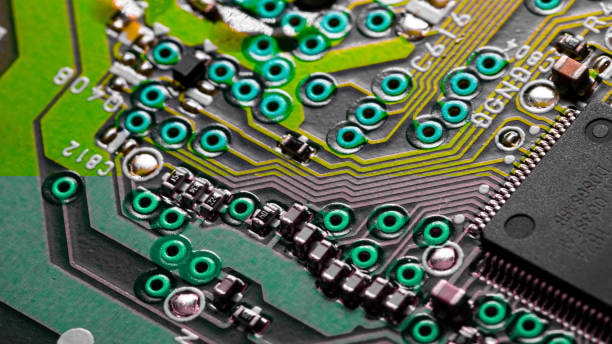
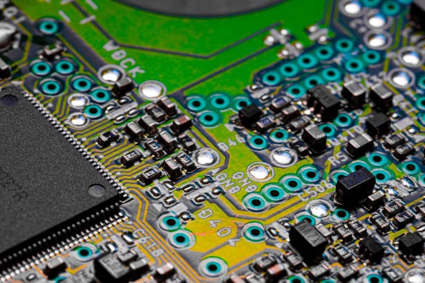
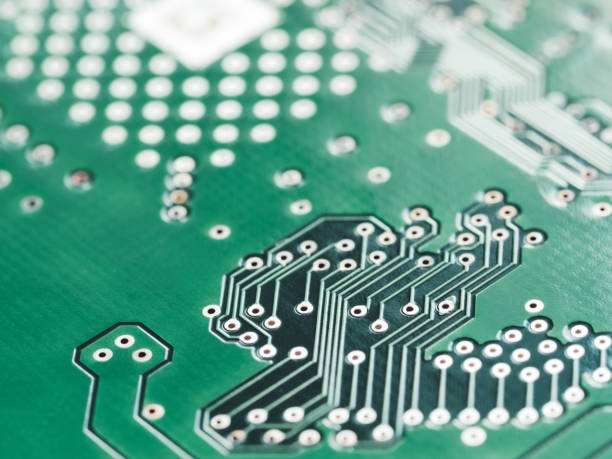
Vias are holes that are drilled on the PCB in a minimal size to allow connections between various layers of the PCB. It is with this knowledge that they are filled with conductive materials to ensure that they act as pathways for these electrical signals. The Pad-in-Via and the Dog Bone structure are especially important for HD and HP PCBs among them. There are various types of vias, each serving different purposes based on the design requirements:
Through-Hole Vias
These are continuous through the entire length of the board and are interconnected on different layers.
Blind Vias
These join an outer layer to one or more inner layers but do not run through the entire board; more typically, they reach down only to an outer layer.
Buried Vias
These interconnect inner layers but do not go beyond them.
What is Via-in-Pad?
Via in pad is a technique where vias are fitted directly under SMDs such as BGAs and CSP devices. Different from other vias where they are interposed between the components, Via-in-Pad actually incorporates the via directly on the pad solution to minimize size and boost electrical specifications.
Benefits of Via-in-Pad
- Space Optimization: With the help of this approach, the through does not protrude away from the component pad and its size can be substantially minimized.” This is particularly true for the high-density interconnect (HDI) arrangements where PCB space is a valuable commodity.
- Improved Signal Integrity: Miniaturization affects the physical size and layout of the interconnects, and Via-in-Pad reduces the distance between the component and the passage way, minimizing signal loss. This is particularly relevant in high-wear applications The term ‘high wear application’ may seem obvious, but it is often used when referring to engineering applications where the object experiences heavy usage in its daily working environment.
- Thermal Management: PowerSEM can increase thermal dispersion through thermal connection between a component and the PCB’s internal layers or thermal layer. This is useful in handling heat produced by power components such as processors by conducting heat away.
- Manufacturing Simplicity: Due to the reduction of the number of trace routes and the layout it is associated with, Via-in-Pad can help make manufacturing less complex, and this can mean that the costs of manufacturing can be cut and the yield rates can be improved.
Challenges of Via-in-Pad
- Solderability Issues: The presence of via in the pad can be a source of solder wicking where solder flows during reflow into the via, undesirably resulting in weak solder joints. This can be prevented by filling the vias or putting a cap on the vias.
- Increased Cost: Via-in-Pad may necessitate subsequent steps like via filling and planarization which sometimes can be complex and costly thus raising the total cost of the PCB.
- Complex Design Process: As compared to traditional PTH, Via-in-Pad technique needs a well-executed engineering design in order to achieve optimum result in terms of reliability and performance, and this can be quite cumbersome.
Best Practices for Via-in-Pad
- Use Filled and Capped Vias: To counter the effects of solder wicking, it is advisable for the pads that cover a via to be filled with either conductive or non-conductive materials and then overlaid with copper. This gives a less curved and perfectly smooth surface that allows soldering of the component.
- Thermal Relief Pads: Avoid or minimize its use for components that are heat sensitive; use thermal relief pads to address the heat dissipation adequately.
- Simulation and Testing: Simplified, it means that through the proper exploitation of the property of Via-in-Pad, it is possible to achieve reliable circuit board design with greater ease and efficiency; this justifies the need for thorough simulation and testing. Ultrafast converging SI analysis, comprehensive power integrity analysis, and thermal management modeling are important.
- Collaboration with Manufacturers: Have particularly strong interactions with PCB manufacturers such that I can identify what they are capable of or not capable of doing in terms of Via-in-Pad technology. This way one is able to ensure that the design is practical and feasible to manufacture hence enhancing cost effectiveness.
What is Dog Bone Structure?
It is a design technique of PCBs in particular BGA where it is a pattern that links the component pads to the via commonly referred to as Dog Bone structure. It involves formation of short trace that is called the ‘bone’, which is a trace that runs from the pad to a via which is somewhat offset from the pad. The name credit of “Dog Bone” can be attributed to the fact that, if one joins the pad, the trace, and the via, one ends up with something that resembles a dog bone.
Benefits of Dog Bone Structure
- Simplified Routing: Dog Bone structures are thus used to give a direct access for traces from the more populated BGA parts to vias thus reducing the density and congestion of the layout.
- Enhanced Reliability: Altogether due to placing the via slightly away from the pad, Dog Bone structures provide better protection against solder wicking and all related problems regarding solderability that helps improve the strength of solder joints.
- Improved Signal Integrity: Reducing the distance of the metal trace between the pad and via is also beneficial as it maintains signal quality, which is paramount in high frequency and speed signals.
- Manufacturing Flexibility: Furthermore, Dog Bone structures are easily integrated into factory production as they are not very elaborate to be implemented in comparison to other advanced engineering processes.
Challenges of Dog Bone Structure
- Space Constraints: As effective as Dog Bone structures may be, they are more bulky than Via-in-Pad Designs, hence are more limiting when it comes to layouts that barely accommodate an inch of board space.
- Complexity in High-Density Designs: In very high-density Designs, it becomes a little tricky controlling the transformation of the dog bone traces needed, ample planning and designing is crucial.
- Potential for Crosstalk: Potential issues include having the multiple Dog Bone traces are too close to each other, resulting to crosstalk issues and signal interference.
Best Practices for Dog Bone Structure
- Optimize Trace Lengths: In Keep the Dog Bone scenario, the traces should be limited in length as much as possible in order to reduce interference and signal loss.
- Maintain Adequate Spacing: Minimize the use of parallel runs of Dog Bone traces and cover sufficiently any gaps in between to minimize crosstalk.
- Layer Management: Proper utilization of multiple layers can be helpful in controlling Dog Bone traces particularly in circuits embedded in high density.
- Signal Integrity Analysis: Nested within the mechanical design is Signal Integrity analysis that will prove the design right and check whether the Dog Bone structures have a detrimental effect on the PCB.
Comparing Via-in-Pad and Dog Bone Structures
Space Efficiency
It reveals that structures of Via-in-Pad designs are more compact than Dog Bones thus, making them efficient in terms of space usage. With Via-in-pad technique, the connection is made within the pad itself so that the pad is no more needed as an additional routing space for the connections, which makes it perfect for very small designs.
Signal Integrity
It is possible to employ both Via-in-Pad and Dog Bone structures to improve signal integrity, even though Via-in-Pad is preferable due to the shorter links between all components. Nonetheless, the structures in Dog Bone topologies satisfy good signal integrity and even simpler to implement using conventional production practices.
Manufacturing Considerations
Derived with advanced manufacturing methods like via filling and capping, Via-in-Pad may itself raise costs. On the other hand, Dog Bone structures are more conformable to regular manufacturing applications and are easier and cheaper to develop than the Stone Vane.
Reliability
Indeed, it can be noted that both techniques can offer reliable connections in case of proper design. When not well filled and capped, Via-in-Pad may experiences solder wicking problems and more so Dog Bone structures requires enough space between them to avoid crosstalk.
When to Use Via-in-Pad
- High-Density Designs: Via-in-Pad is particularly useful for designs that need to incorporate large LED displays into a small form factor possible in today’s smartphones, wearables, and portable electronics.
- High-Frequency Applications: For models used in strict signal environments like RF and microwave, Via-in-Pad is immensely beneficial and performs well.
- Thermal Management: Implement the Via-in-Pad for those components which need to dissipate heat for efficient operation.
When to Use Dog Bone Structures
- Standard Density Designs: Dog Bone structures are best for designs that are not limited in board space like PCBs are in their applications with industrial and automotive use.
- Cost-Sensitive Projects: But for those who financially cant afford the Via-in-Pad, Dog Bone structures are cheaper structures to be implemented in a project.
- Simpler Manufacturing: Thus, structures based on the Dog Bone concept ensure the maintenance of stability and strength when it is impossible or inexpedient to use more advanced forms of manufacturing.
Conclusion
Both Via-in-Pad and Dog Bone structures should be appreciated and applied in PCB design improvement, mainly in the context of highly dense and high-performance designs. Via-in-Pad is more effective in space management compared to regular via and provides better signal quality, though its implementation is costly and time-consuming compared to the other methods above. Dairy dog designs are relatively cheaper and easier to construct than the DB structures, despite offering good performance and reliability.
It is important to adhere to such guidelines and always evaluate and analyze each project in order to harness these complicated methods in order to produce proficient, solid, and high-performance PCB. This means the designs can only be achieved through collaboration with the manufacturers of PCBs and simulation and testing of the designs is paramount. These technologies are likely to remain integral with growth of other electronic products; thus, applying these techniques will be critical as developers seek to remain relevant in evolving markets.