


Erik Hosler Highlights the Role of Quantum Metrology in Advancing Semiconductor Technologies
 Erik Hosler Highlights the Role of Quantum Metrology in Advancing Semiconductor Technologies
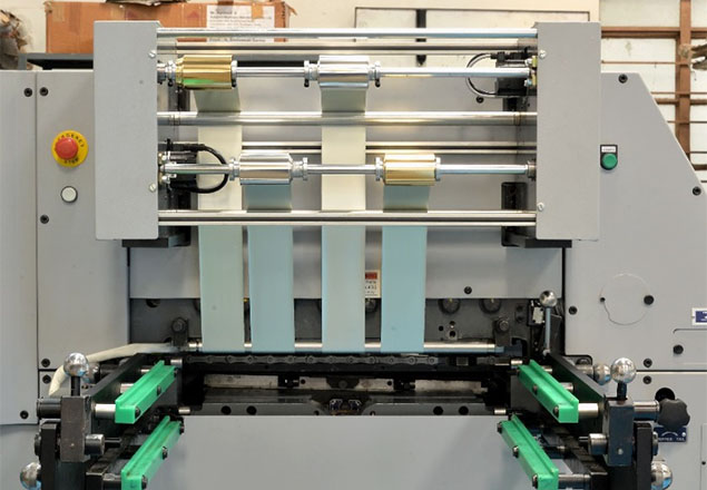
As semiconductor manufacturing reaches the atomic scale, traditional measurement techniques struggle to maintain the precision required for next-generation chips. Quantum metrology, which leverages the principles of quantum mechanics to enhance measurement accuracy, is emerging as a game-changer for the industry. Erik Hosler, a specialist in advanced metrology techniques and semiconductor innovation, mentions that quantum-based measurement tools are setting new standards for precision, reliability and scalability in chip fabrication.
Why Quantum Metrology is Essential for Semiconductor Manufacturing
Modern semiconductor devices, particularly those used in artificial intelligence (AI), high-performance computing (HPC) and 3D-integrated circuits (3D ICs), require precise control at the atomic level. Conventional metrology tools, while effective for larger geometries, face limitations when measuring nanoscale defects, line-edge roughness and material variations.
Quantum metrology overcomes these challenges by utilizing quantum states—such as entanglement and superposition—to measure physical properties with extreme precision. These techniques enable manufacturers to achieve sub-nanometer accuracy, which is critical for improving chip performance, reducing power consumption and increasing yield rates.
Quantum Sensors: Unlocking Unprecedented Accuracy
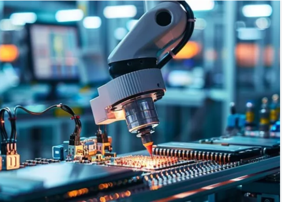
One key advancement in quantum metrology is the development of quantum sensors. Unlike traditional sensors, which rely on classical physics, quantum sensors exploit atomic and subatomic properties to detect minute variations in electrical fields, strain and temperature.
For instance, diamond nitrogen vacancy (NV) centers are being used to detect material defects in semiconductor wafers with unparalleled sensitivity. These quantum-based sensors provide real-time, high-resolution imaging of nanoscale structures, allowing fabs to identify and correct defects early in the production process.
Free-electron lasers and Quantum Light Sources
Next-generation semiconductor inspection tools are also benefiting from quantum-based light sources. Erik Hosler stresses,“Free-electron lasers (FELs) will revolutionize defect detection by offering unprecedented accuracy at the sub-nanometer scale.” These high-intensity, tunable light sources provide sharper imaging and deeper penetration, making them ideal for analyzing buried defects in multilayer semiconductor structures.
By integrating FELs into metrology systems, fabs can improve inspection accuracy, enhance production yields and reduce waste. This capability is particularly valuable in the fabrication of 3D-stacked chips, where detecting interlayer inconsistencies is a major challenge.
The Future of Quantum Metrology in Semiconductors
As semiconductor devices continue to shrink, quantum metrology will play an increasingly vital role in ensuring their performance and reliability. The ability to measure at unprecedented levels of accuracy will refine current manufacturing processes and enable breakthroughs in quantum computing, neuromorphic chips and next-generation transistors.
By leveraging quantum mechanics, the semiconductor industry is entering a new era of precision and innovation, where manufacturing at the atomic level is no longer a challenge but an opportunity for progress.